Table of Contents
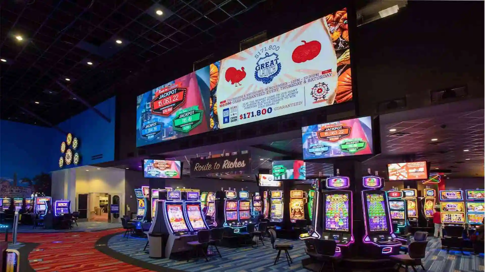
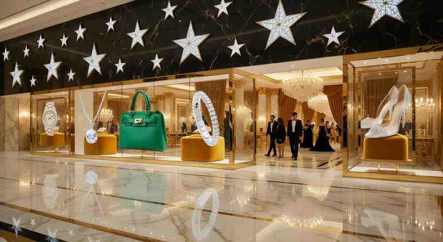
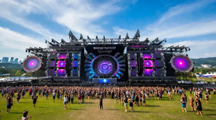
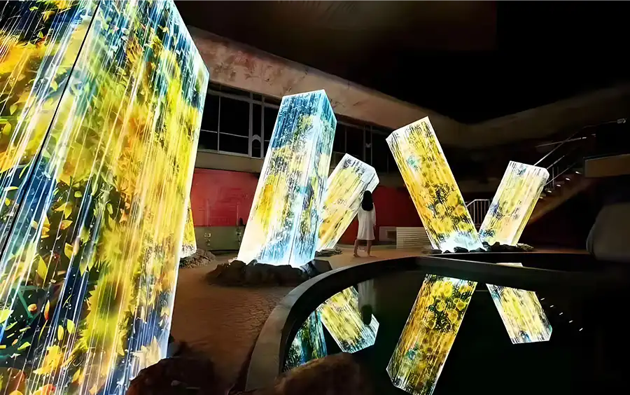
Hot Recommendations
Get a Free Quote Instantly!
Talk to Our Sales Team Now.

Modern LED Display Screens rely on semiconductor electroluminescence, where InGaN/GaN chips emit blue light (450nm) converted to white via phosphor coating. High-end displays achieve 16-bit grayscale, 3840Hz refresh rates, and 5,000 nits brightness for outdoor applications.
Type: InGaN blue chips (2835/1010 packages)
Specifications:
Wavelength: 450±2nm
Forward Voltage: 2.8-3.4V @20mA
Luminous Efficacy: ≥180 lm/W
| Material | Properties | Application |
|---|---|---|
| Epoxy Resin | Refractive Index 1.53, ΔYI <2 | LAMP LEDs |
| Silicone | Transmittance 95%, CTE 250ppm | SMD/Mini LEDs |
| EMC | Halogen-free, TG 150℃ | Automotive Displays |
Aluminum PCB: Thermal conductivity ≥2.2W/m·K, Cu thickness 35±5μm
Ceramic PCB: AlN substrates (24W/m·K) for high-power LED arrays
Adhesive: Silver epoxy (80% Ag content)
Curing: 150℃/1hr, bond line thickness 25±5μm
Accuracy: Placement error ≤±15μm
Wire: 99.99% Au, diameter 1.0mil
Parameters: Ultrasonic power 50W, force 30g, cycle time 0.3s
Process: Vacuum potting (≤1kPa, 30min degassing)
Curing: 135℃/4hrs, bubble diameter ≤30μm
Pin Forming: Shear cutting ±0.1mm tolerance
Binning: Wavelength ±2nm, luminous intensity ±5%
Stencil: Laser-cut stainless steel, 0.12mm thickness
Solder: SAC305 alloy, volume 80-120μm (SPI monitored)
Machine: High-speed pick-and-place (30,000 CPH)
Precision: ±0.03mm (X/Y), ±0.5° (θ)
Profile:
Preheat: 1-2℃/s to 150℃
Peak: 245℃ (60s above 217℃)
Atmosphere: Nitrogen (O₂ <1,000ppm)
Molding: Transfer process @8-12MPa, 150℃/180s
Laser Cutting: 355nm UV laser, 5W power, 100mm/s speed
Laser Lift-Off (LLO):
Transfer rate: 99.99% (R&D), 99.9% (production)
Accuracy: ±1.5μm placement
Pixel Density: 100-200 PPI
Encapsulation: Black epoxy fill (ΔE <1.5)
AEC-Q102: -40℃ to 125℃ operation, 85℃/85%RH/1,000h
Vibration Test: 50G shock (MIL-STD-883 Method 2002)
AOI: Defect detection ≥99.9% (solder bridges, missing parts)
X-Ray: Voiding <15% in solder joints
| Test | Conditions | Requirements |
|---|---|---|
| Thermal Cycling | -40℃ ↔85℃, 1,000 cycles | Lumen maintenance ≥97% |
| Salt Spray | 5% NaCl, 96h | Corrosion area ≤3% |
| HAST | 130℃/85%RH, 96h | IR ≥100MΩ |
Integrating Sphere: CCT tolerance ±150K, CRI ≥80
Viewing Angle: ≥140° horizontal/vertical, ≤50% brightness drop
MSL Level: Level 3 (72hrs floor life @30℃/60%RH)
Dry Packaging: <10% RH with desiccant
ISTA 3A: Survives 1.2m drops, 50G impacts
Safety: UL/cUL, CE, CCC
Environmental: RoHS 2.0, REACH SVHC <0.1%
If you are interested in our products, please contact us promptly
Reach out to our sales team to explore customized solutions that perfectly meet your business needs and address any questions you may have.
Email Address:info@reissopto.comFactory Address:Building 6, Huike Flat Panel Display Industrial Park, No. 1, Gongye 2nd Road, Shiyan Shilong Community, Bao'an District, Shenzhen city , China
whatsapp:15217757270